- 您现在的位置:买卖IC网 > Sheet目录2005 > LTC2255CUH#TRPBF (Linear Technology)IC ADC 14BIT 125MSPS 3V 32-QFN
LTC2255/LTC2254
3
22554fa
LTC2255
LTC2254
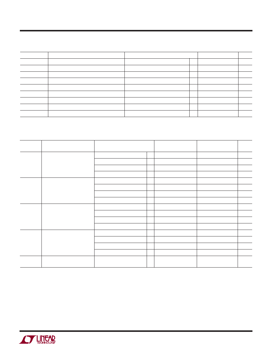
SYMBOL
PARAMETER
CONDITIONS
MIN
TYP
MAX
MIN
TYP
MAX
UNITS
SNR
Signal-to-Noise Ratio
5MHz Input
72.4
72.5
dB
30MHz Input
72.3
72.4
dB
70MHz Input
●
68.9
72.1
69.4
72.3
dB
140MHz Input
71.7
dB
SFDR
5MHz Input
88
dB
30MHz Input
85
88
dB
70MHz Input
●
73
82
71
84
dB
140MHz Input
78
80
dB
SFDR
5MHz Input
90
dB
30MHz Input
90
dB
70MHz Input
●
77
90
79
90
dB
140MHz Input
90
dB
S/(N+D)
5MHz Input
72.2
72.4
dB
30MHz Input
72
72.2
dB
70MHz Input
●
68
71.9
68.5
72
dB
140MHz Input
70.2
70.6
dB
IMD
Intermodulation
fIN1 = 28.2MHz
85
dB
Distortion
fIN2 = 26.8MHz
SYMBOL
PARAMETER
CONDITIONS
MIN
TYP
MAX
UNITS
VIN
Analog Input Range (AIN+ –AIN–)
2.85V < VDD < 3.4V (Note 7)
●
±0.5V to ±1V
V
VIN,CM
Analog Input Common Mode
Differential Input (Note 7)
●
1
1.5
1.9
V
IIN
Analog Input Leakage Current
0V < AIN+, AIN– < VDD
●
–1
1
A
ISENSE
SENSE Input Leakage
0V < SENSE < 1V
●
–3
3
A
IMODE
MODE Pin Leakage
●
–3
3
A
tAP
Sample-and-Hold Acquisition Delay Time
0
ns
tJITTER
Sample-and-Hold Acquisition Delay Time Jitter
0.2
psRMS
CMRR
Analog Input Common Mode Rejection Ratio
80
dB
Full Power Bandwidth
Figure 8 Test Circuit
640
MHz
The
● denotes the specifications which apply over the full operating temperature range,
otherwise specifications are at TA = 25°C. AIN = –1dBFS. (Note 4)
A ALOG I PUT
U
DY A IC ACCURACY
U
W
The
● denotes the specifications which apply over the full operating temperature range, otherwise
specifications are at TA = 25°C. (Note 4)
Signal-to-Noise Plus
Distortion Ratio
Spurious Free Dynamic Range
4th Harmonic or Higher
Spurious Free Dynamic Range
2nd or 3rd Harmonic
发布紧急采购,3分钟左右您将得到回复。
相关PDF资料
LTC2258IUJ-12#PBF
IC ADC 12BIT 65MSPS 1.8V 40-QFN
LTC2262CUJ-14#TRPBF
IC ADC 14BIT 150MSPS 40-QFN
LTC2262IUJ-12#PBF
IC ADC 12BIT 150MSPS 40-QFN
LTC2264CUJ-12#PBF
IC ADC 12BIT SER/PAR 40M 40-QFN
LTC2268IUJ-14#TRPBF
IC ADC 14BIT 125MSPS DUAL 40QFN
LTC2280CUP#PBF
IC ADC DUAL 10BIT 105MSPS 64-QFN
LTC2281IUP#PBF
IC ADC 10BIT DUAL 64-QFN
LTC2282CUP#PBF
IC ADC DUAL 12BIT 105MSPS 64-QFN
相关代理商/技术参数
LTC2255IUH
制造商:Linear Technology 功能描述:ADC Single Pipelined 125Msps 14-bit Parallel 32-Pin QFN EP
LTC2255IUH#PBF
功能描述:IC ADC 14-BIT 125MSPS 3V 32-QFN RoHS:是 类别:集成电路 (IC) >> 数据采集 - 模数转换器 系列:- 标准包装:1 系列:microPOWER™ 位数:8 采样率(每秒):1M 数据接口:串行,SPI? 转换器数目:1 功率耗散(最大):- 电压电源:模拟和数字 工作温度:-40°C ~ 125°C 安装类型:表面贴装 封装/外壳:24-VFQFN 裸露焊盘 供应商设备封装:24-VQFN 裸露焊盘(4x4) 包装:Digi-Reel® 输入数目和类型:8 个单端,单极 产品目录页面:892 (CN2011-ZH PDF) 其它名称:296-25851-6
LTC2255IUH#TR
制造商:Linear Technology 功能描述:ADC Single Pipelined 125Msps 14-bit Parallel 32-Pin QFN EP T/R
LTC2255IUH#TRPBF
功能描述:IC ADC 14BIT 125MSPS 3V 32-QFN RoHS:是 类别:集成电路 (IC) >> 数据采集 - 模数转换器 系列:- 标准包装:1 系列:- 位数:14 采样率(每秒):83k 数据接口:串行,并联 转换器数目:1 功率耗散(最大):95mW 电压电源:双 ± 工作温度:0°C ~ 70°C 安装类型:通孔 封装/外壳:28-DIP(0.600",15.24mm) 供应商设备封装:28-PDIP 包装:管件 输入数目和类型:1 个单端,双极
LTC2256-12
制造商:LINER 制造商全称:Linear Technology 功能描述:12-Bit, 65/40/2 5Msps Ultralow Power 1.8V ADCs
LTC2256-14
制造商:LINER 制造商全称:Linear Technology 功能描述:14-Bit, 65/40/25Msps Ultralow Power 1.8V ADCs
LTC2256CUJ-12#PBF
功能描述:IC ADC 12BIT 25MSPS 1.8V 40-QFN RoHS:是 类别:集成电路 (IC) >> 数据采集 - 模数转换器 系列:- 标准包装:1,000 系列:- 位数:12 采样率(每秒):300k 数据接口:并联 转换器数目:1 功率耗散(最大):75mW 电压电源:单电源 工作温度:0°C ~ 70°C 安装类型:表面贴装 封装/外壳:24-SOIC(0.295",7.50mm 宽) 供应商设备封装:24-SOIC 包装:带卷 (TR) 输入数目和类型:1 个单端,单极;1 个单端,双极
LTC2256CUJ-12#TRPBF
功能描述:IC ADC 12BIT 25MSPS 1.8V 40-QFN RoHS:是 类别:集成电路 (IC) >> 数据采集 - 模数转换器 系列:- 标准包装:1,000 系列:- 位数:12 采样率(每秒):300k 数据接口:并联 转换器数目:1 功率耗散(最大):75mW 电压电源:单电源 工作温度:0°C ~ 70°C 安装类型:表面贴装 封装/外壳:24-SOIC(0.295",7.50mm 宽) 供应商设备封装:24-SOIC 包装:带卷 (TR) 输入数目和类型:1 个单端,单极;1 个单端,双极